The world of artificial intelligence is defined by exponential growth. The models are getting bigger, the data sets are expanding, and the demand for computational power is insatiable.
To meet this demand, NVIDIA has unveiled its next-generation data center architecture, a monumental leap in computing power designed to be the engine for this new era.
Welcome to Blackwell.
1. What is NVIDIA Blackwell? The Engine of a New Industrial Revolution
NVIDIA Blackwell is the successor to the incredibly successful Hopper architecture (H100/H200 GPUs). It represents a fundamental redesign of the GPU, built from the ground up to tackle the immense challenges of training and running trillion-parameter AI models, massive scientific simulations, and complex data analytics. CEO Jensen Huang has called it the engine to power a “new industrial revolution,” where factories of the future will generate intelligence.
The architecture is named in honor of David Blackwell (1919-2010), a brilliant American mathematician and statistician who made significant contributions to game theory, probability theory, and information theory. His work focused on understanding complex systems and making optimal decisions with incomplete information—a fitting parallel to the goals of modern AI.
While its technology will eventually influence consumer products, Blackwell is designed specifically for:
- AI Researchers and Data Scientists
- Hyperscale Cloud Providers
- High-Performance Computing (HPC) centers
- Enterprise companies building proprietary AI models
2. The Core Innovation: A “Two-for-One” GPU Design
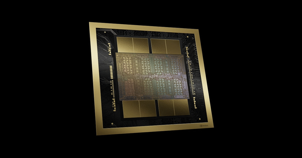
For years, chip designers have been pushing against the “reticle limit”—the maximum physical size of a single piece of silicon that can be manufactured. To overcome this, Blackwell introduces a revolutionary multi-die chiplet architecture.
Instead of one large chip, a Blackwell GPU is composed of two massive dies fused together. These are not two separate GPUs working in parallel; they are designed to function as a single, unified, coherent processor.
- The “NV-HBI” (High-Bandwidth Interface): This is the magic that connects the two dies. The NVIDIA High-Bandwidth Interface provides a staggering 10 terabytes per second (TB/s) of bandwidth between the two chips. This connection is so fast and seamless that the CUDA programming model sees both dies as a single, unified GPU, requiring no special coding to utilize its full power.
- Why More Transistors Matter: This design allows for an astonishing 208 billion transistors on a single Blackwell GPU—more than 2.5 times the 80 billion on the previous Hopper architecture. More transistors directly translate to more processing cores, more specialized engines, and ultimately, more computational power.
3. The Six Pillars of Blackwell: Key Technological Breakthroughs
Blackwell’s performance comes from six key, interconnected innovations that deliver massive gains in compute power, speed, and reliability.
Pillar 1: Second-Generation Transformer Engine
Large Language Models (LLMs) are based on the “Transformer” architecture. Blackwell’s new engine dramatically accelerates these models by using a new, lower-precision number format. It adds support for 4-bit floating point (FP4) and 6-bit floating point (FP6) AI inference. This allows the GPU to perform more calculations with the same amount of memory, doubling the effective compute performance and model size that can be handled.
Pillar 2: Fifth-Generation NVLink
As AI models are scaled across hundreds or thousands of GPUs, the communication speed between them becomes a critical bottleneck. The fifth-generation NVLink provides an unprecedented 1.8 TB/s of bidirectional bandwidth per GPU. This allows up to 576 GPUs to communicate at high speed, enabling the efficient training of the largest and most complex AI models.
Pillar 3: The RAS Engine
RAS stands for Reliability, Availability, and Serviceability. As AI factories run for weeks or months on end, preventing downtime is essential. Blackwell includes a dedicated engine at the chip level for diagnostics and reliability. It can identify potential faults early and help manage the health of a massive GPU cluster, ensuring maximum uptime.
Pillar 4: Secure AI
Protecting an AI model’s intellectual property and the sensitive data it’s trained on is paramount. Blackwell introduces Confidential Computing capabilities at the hardware level. This shields data and models while they are in use, without compromising performance, enabling secure collaboration on sensitive data sets.
Pillar 5: Decompression Engine
Data analytics and database queries are often bottlenecked by the speed at which data can be decompressed from storage into the GPU’s memory. Blackwell features a dedicated decompression engine that can process data at up to 800 GB/s, accelerating these workflows by an order of magnitude compared to CPUs alone.
Pillar 6: The World’s Most Powerful Chip
When all these technologies combine, a single Blackwell GPU can deliver up to 20 petaflops of AI horsepower. This massive leap in raw compute enables tasks that were previously impossible, cementing Blackwell’s status as the most powerful AI processor built to date.
For a great visual overview of the Blackwell journey, from raw silicon to a full data center, check out this video from NVIDIA:
4. Blackwell vs. Hopper: A Generational Leap Forward
The jump from the Hopper to the Blackwell architecture is one of the largest in NVIDIA’s history.
| Feature | Hopper Architecture (H100) | Blackwell Architecture (B200) | Generational Leap |
|---|---|---|---|
| Transistors | 80 Billion | 208 Billion | 2.6x More |
| AI Performance | Up to 4 Petaflops (FP8) | Up to 20 Petaflops (FP4) | 5x More |
| Memory Type | HBM3 | HBM3e | Faster and More Efficient |
| Memory Capacity | Up to 141 GB (H200) | 192 GB | 1.36x More |
| Memory Bandwidth | Up to 4.8 TB/s (H200) | 8 TB/s | 1.67x More |
| NVLink Bandwidth | 900 GB/s (4th Gen) | 1.8 TB/s (5th Gen) | 2x More |
| Energy Efficiency | Baseline | Up to 25x Reduction in Cost & Energy | Massive Improvement |
This table shows that Blackwell isn’t just an incremental update; it’s a fundamental re-architecture that delivers massive gains across every key metric.
5. The Blackwell Product Family: From Single GPUs to Supercomputers
Blackwell is not a single product but a platform that powers a range of solutions designed for different scales.
- The B100 and B200 GPUs: These are the foundational Tensor Core GPUs that can be integrated by server partners like Dell, HPE, and Supermicro. The B100 is designed to be a drop-in replacement for H100 systems, while the B200 offers the full suite of performance.
- The GB200 Grace Blackwell Superchip: This is a powerhouse module that combines two Blackwell B200 GPUs with one Grace CPU on a single board. This “superchip” creates a unified memory space between the CPU and GPUs for incredibly fast data access.
- The NVL72 System: This is a liquid-cooled, rack-scale solution that acts as a single, massive GPU. It connects 36 Grace CPUs and 72 Blackwell GPUs into one giant computer with 1.8 TB/s of internal bandwidth. It’s a true “AI factory in a box.”
- DGX and HGX Systems: NVIDIA’s own branded DGX systems, known as the gold standard for AI infrastructure, will be upgraded with Blackwell technology, offering pre-configured, optimized solutions for enterprises.
6. Real-World Impact: What Can You Do with Blackwell?
The immense power of Blackwell unlocks capabilities that were previously confined to theory.
- Training and Deploying Trillion-Parameter AI Models: Models with over a trillion parameters, like advanced chatbots or reasoning engines, can now be trained and deployed far more efficiently, making real-time inference a reality.
- Accelerating Scientific Simulation (HPC): Fields like drug discovery, climate science, and quantum computing can run simulations with higher fidelity and in a fraction of the time, accelerating the pace of scientific breakthroughs.
- Building Physically Accurate Digital Twins: Engineers can create real-time, physically accurate digital replicas of complex systems like jet engines, entire factories, or even weather patterns, allowing for continuous testing and optimization in a virtual world.
- Powering the Next Wave of Data Centers: The combination of performance and energy efficiency allows data centers to achieve exascale AI computing without an exponential increase in power consumption.
7. Beyond the Data Center: What Blackwell Means for Future GeForce GPUs
While Blackwell is a data center architecture, the innovations developed for it will inevitably “trickle down” to consumer-grade products. The underlying design principles, manufacturing processes, and improvements to core technologies often form the basis for the next generation of GeForce RTX GPUs.
While purely speculative, we could see future gaming and content creation cards benefit from:
- More efficient core designs.
- Advanced memory systems.
- Next-generation Tensor Cores and RT Cores, leading to even faster DLSS and Ray Tracing performance.
8. The Bottom Line: Why Blackwell is a Game-Changer
NVIDIA Blackwell is more than just a faster chip; it represents a significant architectural shift designed to meet a moment of explosive AI growth. By breaking through the physical limits of chip manufacturing with its multi-die design and creating a holistic system with interconnected technologies like NVLink and a new Transformer Engine, NVIDIA has redefined what a supercomputer can be.
Blackwell provides the computational foundation necessary for the next wave of AI, from massive language models to complex scientific simulations. It is the engine that will power the AI factories of tomorrow, turning raw data into world-changing intelligence.
For more technical details, you can visit the Official NVIDIA Blackwell Architecture Page.